Group Stock Code:688328
Service hotline:
+86 0752-5880-900(8280)Group Stock Code:688328
Service hotline:
+86 0752-5880-900(8280)On September 6, 2022, the U.S. Department of Commerce issued the 2022 Chip and Technology Act, which aims to cut off the supply of advanced semiconductor chip technology, equipment and materials to China, accelerate the return of the chip industry to the United States through subsidies, isolate China's chip industry from the world, and reshape the global chip industry chain supply chain pattern.
In the short term, this "Chip Act" involves high-end OEM of advanced manufacturing technology, memory and downstream industries such as consumer electronics and automobiles, which has a great impact on China. In the long run, the domestic substitution of key semiconductor materials has been the consensus of the domestic semiconductor industry. The restrictions of the Act will only accelerate the process of domestic substitution of China's semiconductor industry. At present, the overall localization rate of semiconductor wafer materials is still low, and the domestic substitution task is arduous, but the prospect is broad. Domestic leading enterprises may usher in golden opportunities for development, while the quantity/testing equipment is one of the links with the lowest localization rate, and the localization rate will still be less than 10% in 2022.
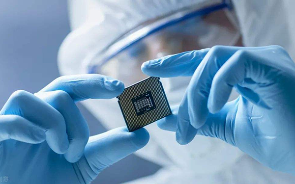
The semiconductor quantity/detection equipment is widely used in the front and back track production of integrated circuits. It is the cornerstone to ensure the precise realization of wafer lithography, etching, film deposition and other links, and is crucial for the silicon wafer factory/wafer factory to ensure product yield, product consistency, and reduce costs.
According to different application scenarios, measurement/detection equipment is mainly divided into measurement and detection, of which detection equipment accounts for 63%.
1) Detection equipment: mainly used to detect whether there is heterogeneity in the wafer structure, such as particle pollution, surface scratch, open and short circuit and other characteristic structural defects;
2) Measuring equipment: it refers to the quantitative description of the structure size and material characteristics of the observed wafer circuit, such as the measurement of physical parameters such as film thickness, key dimensions, etching depth, surface morphology, etc.
According to the technical principles, quantity/detection equipment can be divided into three categories: optics, electron beam and X-ray, of which optics accounts for up to 75%.
1) Optics: It is less destructive to the wafer, and has the advantages of batch and rapid detection. It is widely used in the detection of impurities, particles, pattern defects, etc. on the wafer surface, as well as the measurement of film thickness, key dimensions, engraving accuracy, surface morphology, etc;
2) Electron beam: the precision is higher than that of optical technology, but the speed is slow, which is suitable for spot check of some core processes;
3) X-ray: strong penetrability, nondestructive detection, applicable to a few special scenes such as ultra-thin film measurement, specific metal composition detection, etc.
According to relevant data, the global total sales of measuring equipment in 2020 will be 7.65 billion US dollars, and the five-year CAGR will be 12.6%, of which the proportion of testing equipment will be 62.6%, and the proportion of measuring equipment will be 33.5%
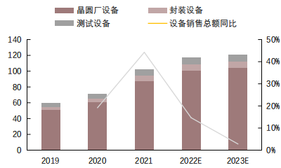
It is worth noting that although the localization rate of detection and measurement equipment in China is low and most of the market is monopolized by Kelei, Applied Materials, Hitachi and other U.S. and Japanese manufacturers, benefiting from the demand of countercyclical expansion of domestic wafer factories, it is estimated that the market size of volume/detection equipment in Chinese Mainland will reach 32.6 billion yuan in 2023, including nano pattern wafer defect detection equipment, mask defect detection equipment, key dimension measurement equipment The market scale of patternless wafer defect detection equipment will reach 8, 37, 3.3 and 3.2 billion yuan respectively. The demand for equipment brought about by advanced packaging technology will greatly promote the expansion of the market scale of packaging and testing equipment. With the increase of the complexity of integrated circuits, the market scale of volume/testing equipment will also steadily increase. In the face of such rapidly growing market demand, domestic volume/testing equipment manufacturers are expected to take advantage of the wind of domestic substitution!
Shenzhen Keda Semiconductor is a national high-tech enterprise invested and established by Shenzhen Keda Intelligent Equipment Co., Ltd. Since its establishment, the company has been focusing on the research, development, production, sales and technical services of semiconductor component test sorters. At present, the localization rate of the company's turret test sorter has been at the top of the industry, covering most of the chip form packages on the market, such as QFN, DFN, SOD, SOT, etc., of which the latest high-speed machine SKD962 has achieved 50K in the air. At the same time, high temperature turrets for automotive electronics and other products are also about to be introduced to the market.
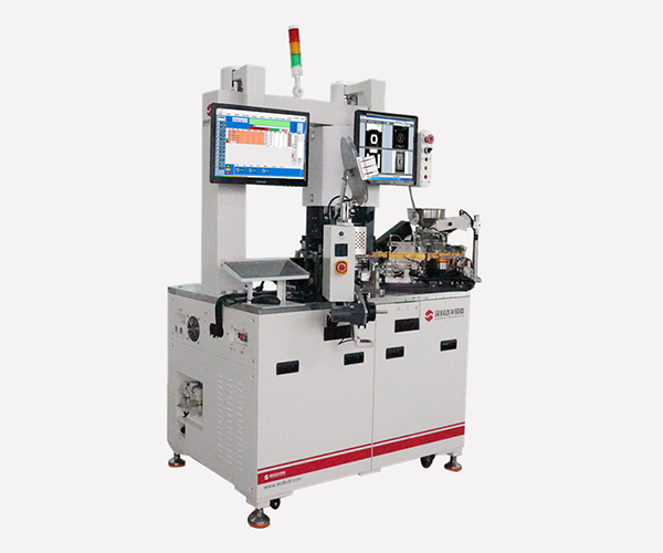
Led by a group of senior personnel in the fields of material application, mechanical transmission, motion logic control, visual computing, semiconductor equipment and automation equipment, Shenzhen Keda Semiconductor is gradually building a bottom technology platform with independent intellectual property rights, and developing various intelligent equipment and intelligent solutions for the semiconductor packaging and testing industry in combination with specific semiconductor processes. At present, the company has more than 50 patents. The next step of research and development will focus on improving the efficiency and stability of existing equipment, and will extend to high-end product lines, such as high and low temperature test sorting, integrated circuit module test sorting, and advanced packaging test sorting.
China's semiconductor industry must adhere to the road of domestic substitution for chip design, front and rear equipment and materials to achieve curve overtaking. This road is doomed to be long, hard and lonely. At the same time, this is a magnificent road that has to go all out. So come on! everybody!