Group Stock Code:688328
Service hotline:
+86 0752-5880-900(8280)Group Stock Code:688328
Service hotline:
+86 0752-5880-900(8280)In the past few decades, chips have been shrinking according to Moore's Law, the size of chips has become smaller and smaller, and the performance has become higher and higher. Because of this, computers that used to be behemoths can become thin and light in our palms, as well as mobile phones, TVs, smart watches, etc., which have brought infinite convenience to our lives. But now, we have encountered obstacles, the speed of transistor miniaturization is slowing down, and Moore's Law is approaching its limit. Chip manufacturers cannot use traditional methods to make smaller circuits at a more economical cost.
So various post-Moore technologies began to be explored. MOSFET transistors entered 3D FinFET from two dimensions and entered GAA; advanced packaging technologies such as 3D packaging and SiP packaging have also become technologies for companies to accelerate the layout, and Chiplet is used. International manufacturers have joined the ranks; new semiconductor materials such as carbon nanotubes are also accelerating their efforts; new storage-computing devices have begun to gradually replace traditional MOS devices; they even have to surpass transistors to enter quantum computing; and so on. The entire semiconductor industry is looking for new ideas for the next development of chips. Now there is a new and more cost-effective technology that may open another door to the miniaturization of chip manufacturing, that is, directed self-assembly technology (DSA), which can be regarded as a complementary technology of photolithography.
At the 2021 SPIE Advanced Lithography Conference, imec, the world’s leading nanoelectronics and digital technology research and innovation center, demonstrated for the first time the ability of directed self-assembly (DSA) to pattern lines/spaces with a pitch as small as 18nm. The optimized dry etching chemistry method successfully transferred the pattern to the underlying thick SiN layer, which will enable further defect detection. These results confirm that Directed Self-Assembly (DSA) has the potential to complement the traditional top-down patterning used in sub-2nm technology node industrial manufacturing.
Before talking about Directed Self-Assembly Technology (DSA), let us first review the current chip manufacturing methods.
Now chips are usually manufactured by photolithography. In short, every tiny feature of the circuit is projected on the silicon wafer. In this process, a photosensitive material called photoresist is coated on the silicon wafer. After that, the silicon wafer will be placed under different patterns, which are formed by light penetrating through filters called masks. Each time the light hits one place, the photoresist will be cured, and the rest will be washed away. In the next step, the wafer is chemically etched to form a functional structure on the exposed part of the surface. The advancement of lithography technology has always been the key to promoting subsequent semiconductor nodes. As the chip enters below 10nm, extreme ultraviolet (EUV) technology is indispensable, lithography has become too complex and costly, and the cost of an EUV lithography machine exceeds 100 million US dollars. In contrast, the cost of chips has also risen accordingly.
In addition to cost, the traditional top-down lithography mode is increasingly being challenged by the inherent problems of photosensitive materials' response to light, such as random printing failure and line edge/line width roughness (LER/LWR). The directed self-assembly (DSA) technology is considered an innovative and more cost-effective manufacturing method, which uses a bottom-up model. As a potential way to supplement and further expand lithography-based patterns.
Directed self-assembly (DSA) uses self-assembled molecules to create nanoscale components of computer chips. Unlike most photolithography techniques that define patterns by masks, it uses block copolymer (BCP) morphology to create lines and spaces And hole patterns help to control the feature shape more accurately. Self-assembly is a method inspired by nature, which can be seen everywhere in nature from lipid membranes to cell structures. The so-called self-assembly refers to the structure of the spontaneous composition of each component, which is the result of specific local interactions between the components, and the structure of their composition is very stable. Industry experts believe that if this method can be used in nature, the same reasoning may also be used in the chip industry.
But in fact, DSA is not a new technology. The industry started its preliminary development as early as 2000. In 2007, DSA was added to the ITRS roadmap. Early supporters believed that DSA would enter the 14nm and 7nm logical nodes. Commercial production has been carried out in the past, but so far, it has not been realized. And now, with the chip technology coming to 7nm, 5nm, 3nm, and the latest development of DSA materials and processing, DSA technology is once again optimistic.
DSA can provide higher resolution than the semiconductor industry currently requires, and feature sizes are now approaching the level at which DSA is particularly effective. If these trends continue, this technology is expected to be widely adopted by the end of this century.
"If you look at integrated circuit structures or transistor arrays, many functional structures are repeated millions of times. This is a highly periodic structure. Therefore, we hope to take advantage of this periodicity in alternative manufacturing techniques and through Assembling materials spontaneously form the periodic structure required by transistors. We use these materials to complete the final fine pattern production work, rather than trying to find a breakthrough in circuit projection technology." said Karl Skjonnemand, director of the semiconductor materials research and development department at Branchburg.
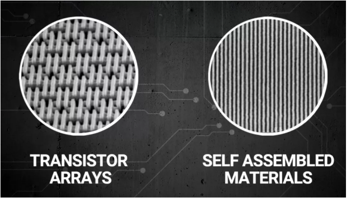
Replace the periodic arrangement of transistors with self-assembled materials (Source: Karl Skjonnemand TED talk)
"The key to self-assembled materials is block copolymers (BCP). These materials are composed of two polymer chains with a length of only tens of nanometers. They have special thermodynamic properties. These two polymer chains hate each other, They are mutually exclusive and incompatible like water and oil, but if we force them to join together, they can form highly regular nanostructures.” Skjonnemand explained, “A giant material may have billions in total. Such polymer chains. Among them, similar polymers will try to bond together, while opposite parts try to separate from each other. Therefore, the polymer chains will move around until they form a fixed shape.
Moreover, the natural self-assembly shape has the characteristics of nanometer level, regularity, periodicity, and long distance, which is exactly what the transistor array needs. So we can use molecular engineering to design transistors of different shapes, sizes and cycles. In other words, by simply adjusting the length and composition of the blocks in the polymer chain, it is possible to produce many different regular patterns and shapes, which can be adjusted to the exact style, size and period according to the design.
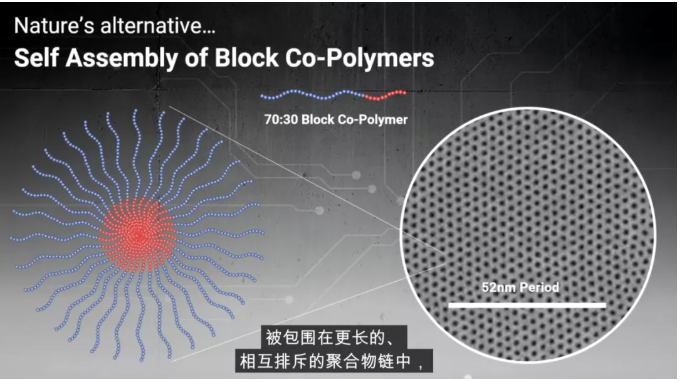
Using self-assembled materials to form different shapes (Source: Karl Skjonnemand TED talk)
The realization of the self-assembly capabilities of these structures is only one part of the manufacturing process leading to the target. Because these structures also need to be arranged so that the transistors can form an integrated circuit. However, the method is relatively simple. It only needs to use a wide guide structure to fix the self-assembled structures, fix them in anchor positions, so that the remaining self-assembled structures can be arranged in parallel, and they can be consistent with the guide structure.
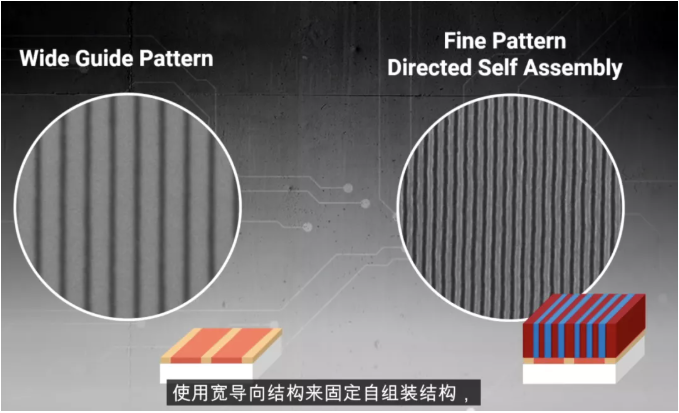
Skjonnemand said, “If we want to make a 40-nanometer thin wire, which is difficult for traditional projection technology, we can use ordinary projection technology to create a 120-nanometer guide structure. This structure will Three 40-nanometer-long lines are arranged together. These materials will take on the most difficult task of fine composition. We call the whole method'directed self-assembly'."
Of course, directed self-assembly is not an independent process, but is integrated with the traditional manufacturing process in order to mass-produce micron and nanostructures at a lower cost. Since traditional photolithography is used in directional self-assembly, another advantage is that manufacturers do not need to invest heavily in new equipment. The pilot project carried out by Branchburg and its customers has shown that compared with traditional multi-reconfiguration drawings, errors in the directional self-assembly manufacturing process are greatly reduced. And they predict that directional self-assembly can reduce the number of process steps involved in manufacturing by more than 40%.
However, there are still some challenges facing directional self-assembly technology to be fully integrated into daily manufacturing. The 2016 DSA seminar survey identified defects as the biggest technical challenge. In Skjonnemand's view, if directional self-assembly is to be used, the entire system needs to be perfectly aligned, because any small defects in the structure may cause transistor failure. Moreover, because there are billions of transistors in the circuit, the system needs to be almost perfect at the molecular level.
Defect rate and cost are directly linked, because the lowest defect level is related to the longest annealing time. Although only five minutes of annealing can separate the two phases, the resulting material contains too many defects and is not suitable for commercial use.
"We will take unconventional measures to achieve this goal." He continued, "By optimally cleaning chemicals in semiconductor factories and carefully handling these materials, we can eliminate even the smallest nanoscale Defects."
At the 2021 SPIE Advanced Lithography Conference, imec, the world’s leading nanoelectronics and digital technology research and innovation center, demonstrated for the first time the ability of directed self-assembly (DSA) to pattern lines/spaces with a pitch as small as 18nm, using high The chi block copolymer (high χ BCP)-based process is under high volume production (HVM) conditions.
But this technology is still in development. Although the semiconductor industry has rich experience in lithography, the use of Directed Self-Assembly (DSA) technology requires a change in the way of thinking. Block copolymer (BCP) materials and processes are revolutionary, not evolutionary. This is not what the industry is used to and may face resistance. And directed self-assembly (DSA) needs to be demonstrated on real equipment before it can succeed in the semiconductor market. Therefore, cooperation between material suppliers in the semiconductor industry and chemical companies with extensive experience in block copolymers (BCP) is one of the ways to bridge this gap.
In this regard, Merck is an expert in the chemical industry. It is reported that Merck's advancements in self-assembly technology have enabled customers to begin planning for high-volume manufacturing capacity. Merck is developing extremely pure high-volume synthesis capabilities to meet customers' pursuit of performance and quality goals.
"This revolutionary technology is expected to revolutionize the semiconductor manufacturing process and will accelerate the introduction of next-generation patterning applications." said Anand Nambiar, global head of Merck Semiconductor Solutions. Merck believes that directional self-assembly can become an advanced manufacturing process in the semiconductor industry in the next few years.
If directed self-assembly can really enter semiconductor manufacturing, the industry will be able to produce smaller and smaller transistors in a more cost-effective manner, thus ensuring that the computing and digital revolution can continue to move forward at an amazing pace Step forward. This also heralds the dawn of a new era of molecular manufacturing.
#humanprogress In recent years, Directed Self-Assembly (DSA) has attracted the interest of a large number of colleagues in the industry and has developed into a valuable ecosystem composed of universities, metrologists, materials and equipment suppliers. Unlike previous efforts in a single industry, the cooperation between materials and chemical companies will better promote the real implementation of directional self-assembly technology. A revolution in chip manufacturing is coming, so how will Merck unite with material manufacturers to use directed self-assembly technology to create forward-looking microchips?
Note: Reprinted from "Semiconductor Industry Observation"
Reprint link: https://mp.weixin.qq.com/s/6WXqjP2CYcqEEmdWGasohg