Group Stock Code:688328
Service hotline:
+86 0752-5880-900(8280)Group Stock Code:688328
Service hotline:
+86 0752-5880-900(8280)The generation of chips will go through several major links, including chip design, wafer manufacturing and packaging test. In fact, in the design phase, the chip has a complete verification process. Simulation verification, UVM, formal verification and FPGA based system level verification (SLE, System Level Emulation) and other verification methods can ensure 100% design function correctness. Generally speaking, the chip can be processed to the streaming stage. The netlist of the chip has been verified by all test cases, and perfectly realizes the design requirements. Therefore, the key point of semiconductor testing is to detect and verify the manufacturing process
The chip manufacturing process is extremely complex, and each step may bring errors that affect the final yield. Therefore, the testing process will be included in the key manufacturing process. Based on the semiconductor manufacturing process and the division of labor in the industry chain, the chip manufacturing process is divided into the former process and the latter process, and the corresponding tests are also divided into the former test and the latter test
1、 Front track test
The former process is mainly the process of wafer manufacturing. It is the process of coating, exposure, development, etching, ion implantation, metal sputtering and other links on the silicon wafer for many times, and finally forms an integrated circuit with overlapping multilayer circuits
Therefore, the object of the previous test is the wafer in the process, and the main test contents can be divided into two aspects:
1. Measurement, mainly measuring chip manufacturing process size, material properties, etc., such as film thickness measurement, OCD size measurement, etc
2. Detection, mainly detecting chip impurities, surface mechanical scratches, wafer pattern defects, etc
The technologies involved in the previous test mainly include materials, optics, microphysics, chemistry, etc. The corresponding test equipment includes film thickness measuring equipment, OCD key dimension measuring equipment, photolithography calibration measuring equipment, graphic defect detection equipment, etc
2、 Rear track test
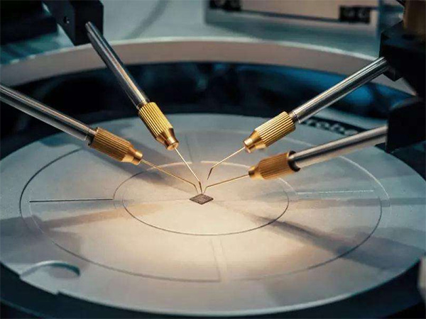
The following process starts with the receipt of a Wafer containing hundreds or thousands of neatly arranged Dies. The main process is to cut, bond and package the Dies. The whole process starts with CP test and ends with FT test
CP test, also known as wafer test, aims to verify whether each die in the whole wafer can basically meet the characteristics or design specifications of the chip. To put it bluntly, it is to conduct acceptance tests on the incoming Wafer to prevent substandard Die from entering the packaging process and reduce packaging cost waste. The test items are mainly for the verification of functional and electrical parameters
FT test is the last interception before the chip leaves the factory. The object of FT test is the encapsulated chip, and the main goal is to avoid the direct outflow of the chip that causes damage during Wafer cutting or leads to abnormal bonding after cutting. The main test content of FT test is also functional and electrical parameter test
It is worth noting that the test items of CP test and FT test are similar. Some of their test instruments can even be the same type. However, because the test objects are at different stages of the chip and the loading and connection methods are different, different supporting equipment is required. What are the functional tests and electrical tests to be performed by the test instrument as the core part? Generally, it mainly includes three aspects of testing:
DC parameter test: mainly measure the voltage and current parameters under various conditions to verify whether the chip meets the design specifications, such as open/short circuit, leakage current, etc
AC parameter test: mainly test the timing related indicators to verify whether the chip meets the design specifications, such as transmission delay, signal rise/fall time, etc
Function test: mainly test the logic operation, signal processing, control, storage, transmission, etc. of the chip